
A single bit of dust can ruin a wafer worth thousands of dollars.
That’s the reason semiconductor manufacturing operates under conditions most factories never have to consider. Air stays continuously filtered. Workers suit up head to toe before they even step through the door. Equipment gets built around contamination control from the ground up. And materials have to move between hundreds of tightly controlled process steps without picking up particles, damaging a wafer, or losing track of what went where.
This is exactly where cleanroom robotics in semiconductor manufacturing earns its place.
India is shifting from a country that imported nearly every chip it used to one building its own semiconductor manufacturing and packaging ecosystem. New fabs, OSAT facilities, and electronics manufacturing plants are taking shape right now, and automation is getting designed into these factories from day one, not added later.
For these facilities, robotics is about hitting the precision, repeatability, traceability, and contamination control that advanced manufacturing simply demands.
What Cleanroom Robots Do
A single wafer may undergo hundreds of process steps, and each stage calls for careful handling. Even a small amount of contamination or a small error in the transfer process can have downstream effects on the end product.
Cleanroom robots are built specifically to operate in this environment.
Depending on the application, they handle the following:
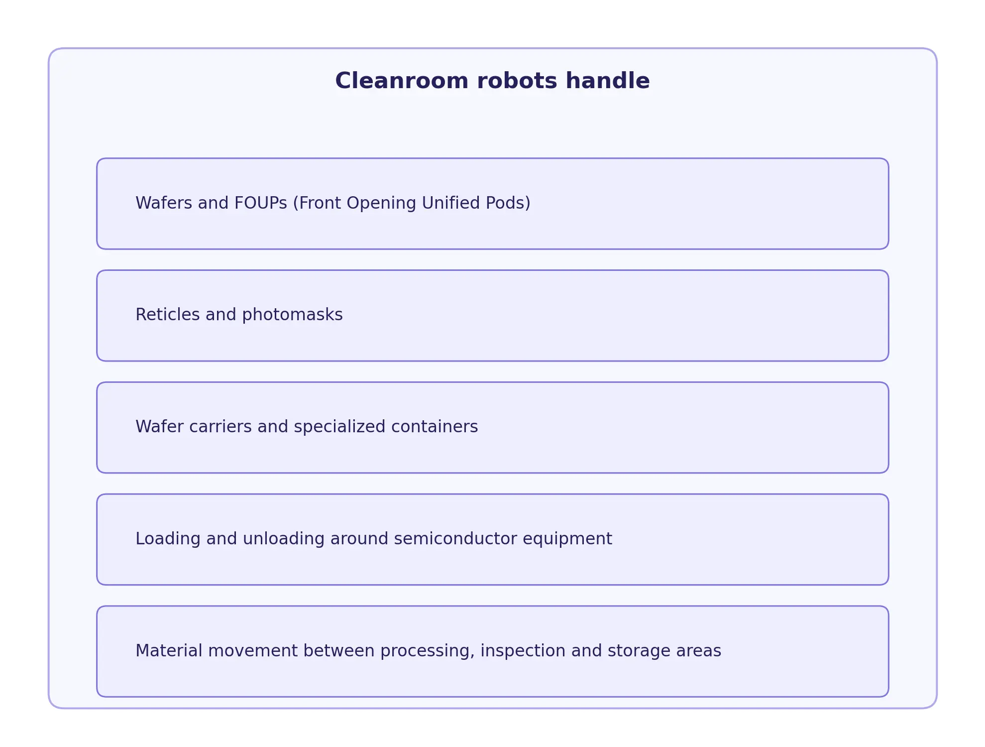
A robot repeats the same movement thousands of times over while keeping human intervention to a minimum. Semiconductor-grade robotic systems can also be built for highly controlled cleanroom and vacuum environments, depending on the specific application and qualification requirements involved.
That level of control matters more and more as manufacturers scale up production. According to MarketsandMarkets, the robotic arms and cleanroom robots segment is forecast to post the fastest growth of any category in the global semiconductor cleanroom market through 2030.
Why Semiconductor Automation in India Is Picking Up Speed
India’s semiconductor story has moved well past the policy-announcement stage.
Under the India Semiconductor Mission, the government has approved projects spanning semiconductor fabrication, display manufacturing, and packaging.
As of the most recent Cabinet approvals, that’s 12 projects across six states, with cumulative investments of around ₹1.64 lakh crore, as per PIB. Of those 12, one is a full semiconductor fabrication unit, two are compound-semiconductor fabs, and the remaining nine are packaging and testing (OSAT/ATMP) facilities, a mix worth keeping in mind, since fab-floor automation and packaging-line automation don’t always call for the same equipment or the same qualification standards.
But standing up a fab is never just about installing advanced processing equipment. The factory also needs a dependable way to move materials between all those machines.
That’s where semiconductor automation in India starts to matter.
A modern semiconductor facility has to get the right material to the right location at the right time, all while maintaining environmental controls and full traceability.
Automation gives you a far more controlled way to manage that movement. And it never comes down to just one type of robot.
How Automation Moves Materials Inside a Semiconductor Fab
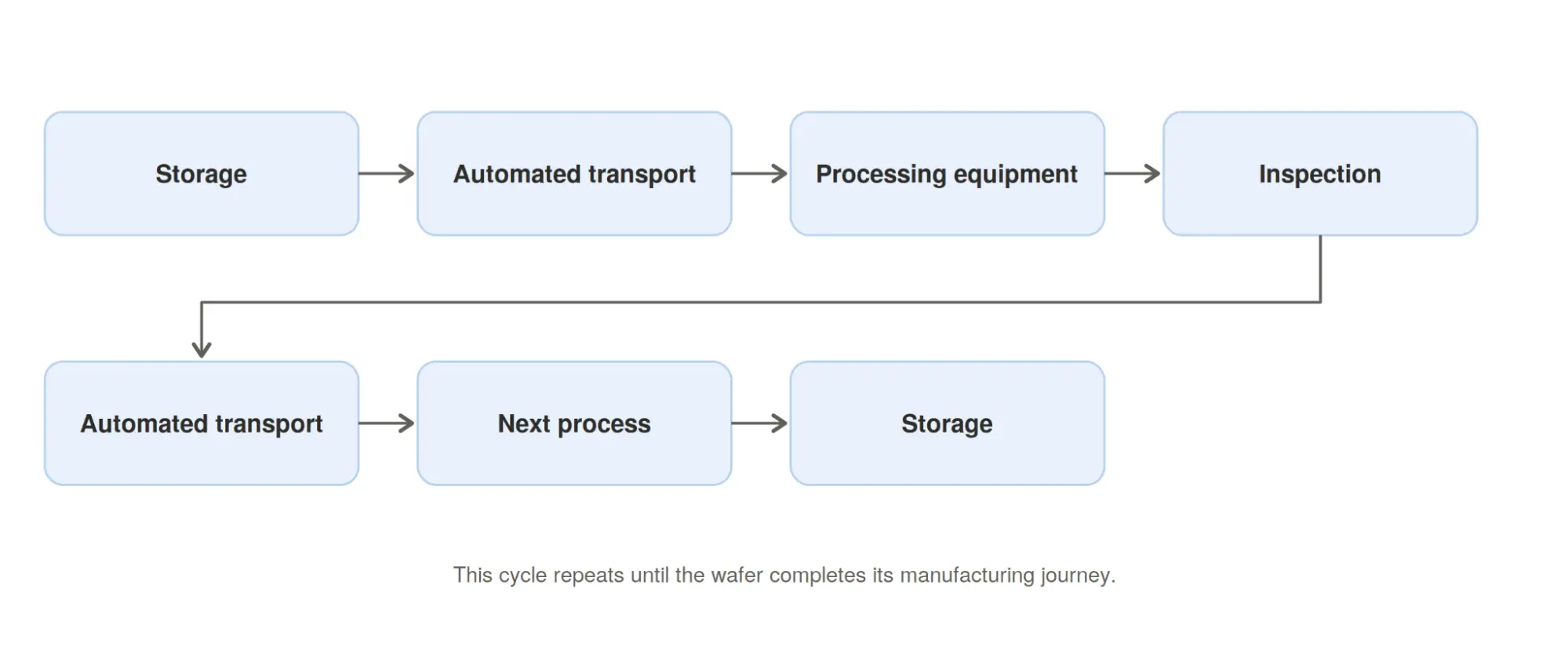
Think about what a single wafer goes through as it moves across the fab.
It begins in storage, then moves to the processing equipment, then through inspection and metrology, and onto the next step. The cycle repeats until the wafer has undergone the entire manufacturing process.
Here is a simple version of that flow:
Different systems handle different legs of that journey:
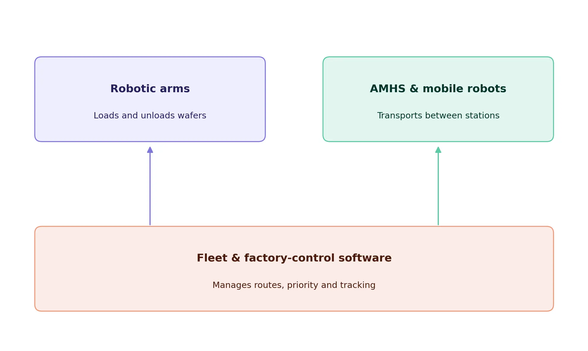
- Robotic arms work around fixed processing equipment. They load and unload wafers, transfer materials between stations, and carry out highly precise, repetitive movements.
- Automated material handling systems and mobile robots cover transportation between equipment, storage areas, and other designated points.
- Fleet and factory-control software ties it all together, managing routes, priorities, equipment availability, and material tracking.
The point is to build an automation architecture where every system has a clearly defined job in keeping production moving.
Why Cleanroom AMRs Need a Different Design Approach
Fixed infrastructure and dynamic floor layouts already push manufacturers toward AMRs built for their specific environment – cleanrooms just take that further. You can’t just take a conventional warehouse AMR, roll it into a semiconductor cleanroom, and expect it to perform.
The environment demands a completely different set of design requirements. Depending on the application, manufacturers need to weigh the following:
- Particle generation and contamination control – every moving part, motor, and surface finish on the robot has to meet the fab’s particle-count standards, since the robot itself can become a contamination source.
- Navigation accuracy – cleanroom layouts are tight and precisely mapped, so the robot needs sub-centimeter positioning to avoid collisions with equipment and other traffic.
- Payload and carrier compatibility – the robot has to handle FOUPs, reticle pods, and other specialized carriers without vibration or tilt that could damage the contents.
- Safety around people and equipment – cleanroom staff, fixed tools, and other robots share the same tight floor space, so collision avoidance and predictable stopping behavior matter more than in an open warehouse.
- Integration with factory-control systems – the robot needs to talk directly to fab scheduling and equipment-availability systems, not operate as an isolated unit.
- Real-time material tracking and traceability – every movement has to be logged against the wafer lot or carrier ID, since fabs need a full audit trail for yield and compliance.
That’s exactly why cleanroom robots rated for this kind of work need to be evaluated as part of the full automation architecture, not as standalone machines bolted on afterward.
Where Electronics Manufacturing Robots Fit Beyond the Fab
The semiconductor opportunity doesn’t stop at wafer fabrication.
India’s ecosystem is also growing across semiconductor packaging, assembly and testing, electronics manufacturing, component production, and other downstream operations. These facilities face many of the same challenges.
Materials need to move predictably between production, inspection, storage, and testing. Work-in-progress has to stay traceable. And manual handling needs to shrink wherever it introduces delay or inconsistency.
This is exactly where electronics manufacturing robots create value well beyond the cleanroom itself.
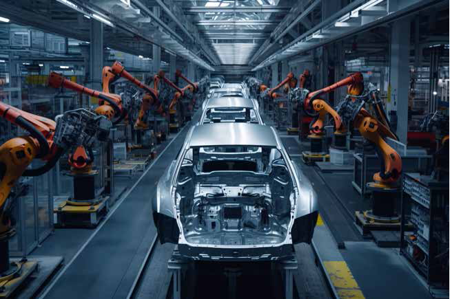
Packaging and testing operations, for instance, often need automated movement of materials across multiple production stages. Electronics manufacturing lines benefit the same way, from autonomous movement of components, work-in-progress, and finished products.
The bigger opportunity here is an interconnected manufacturing ecosystem, one where automation supports material movement across the entire production chain, not just one isolated stage of it.
Where This Leaves You
As fabs, packaging facilities, and electronics manufacturing operations ramp up, it’s automation, not an afterthought bolted onto an already-running line, that keeps material movement precise, repeatable, traceable, and under control.
For manufacturers looking to automate, start with the process, not the robot. What needs to move? Where’s it going? How often? Under what environmental conditions? How much traceability does it actually require? Get those answers first, and the right automation architecture becomes a lot easier to identify.
Novus Hi-Tech deploys AMR and autonomous material handling systems across Indian manufacturing environments – automotive, electronics, pharmaceuticals, and precision industrial applications – where contamination control, traceability, and repeatable precision are operational requirements, not optional features.
For manufacturers building automated material movement into their fab or packaging facility, that deployment experience is worth a conversation. If you’re planning automated material movement for a fab, a packaging unit, or anything else feeding into India’s semiconductor supply chain, that track record is a solid place to start the conversation.